


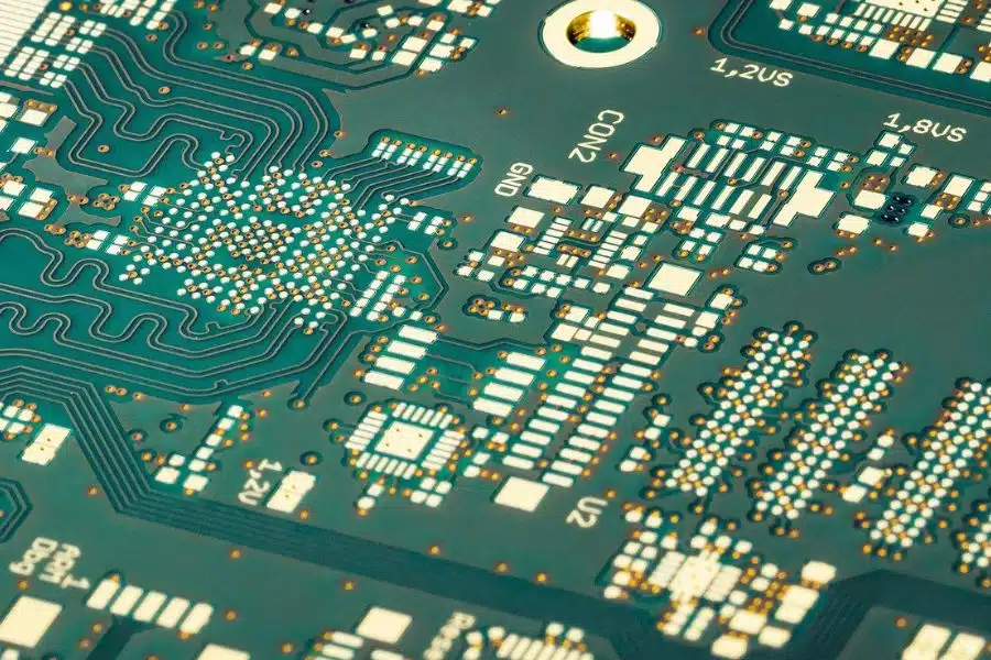
Plenty of engineers see “warpage: pass” on a PCB’s outgoing inspection report and assume that means the board won’t cause problems at assembly. But the inspection report on its own doesn’t actually tell you whether the board will place cleanly on a real SMT line.
Getting a 12-layer complex-system mainboard through SMT assembly successfully takes more than passing impedance and continuity — the electrical metrics. It also requires the stack-up itself to maintain reasonable symmetry in copper distribution and material arrangement. Without that, an inspection report that says “pass” can still fail to stop mass rework at the assembly stage.
What “Warpage: Pass” Actually Means Needs to Be Settled Before Assembly, Not After
When engineers evaluate a 12-layer complex-system board, attention usually goes to electrical metrics — impedance, crosstalk, power integrity. Those tools are genuinely useful for confirming a circuit will work, but they don’t answer a more basic execution question: can this board actually be placed accurately and consistently on the assembly equipment being used?
That’s exactly where “warpage: pass” starts to get ambiguous. The common industry reference for PCB warpage is the IPC-TM-650 test methodology, along with the commonly cited empirical threshold of 0.75% for surface-mount applications. If an inspection report shows warpage within that range, it can genuinely be called “pass” by generic industry standard. But an industry-wide standard is usually a fairly broad empirical reference point, and the real-world assembly process for a specific product — especially a complex-system mainboard with fine-pitch BGAs and a large board area — can have a tolerance for warpage that’s considerably stricter than that generic number.
A team that overlooks this distinction can end up pinning all the blame on the inspection process, without realizing the real issue is the gap hiding behind the word “pass” — the gap between a generic standard and the project’s actual assembly tolerance.
Part One of the Case: The Real Story Behind a Warpage Number
On a 12-layer core processing board built for a data communications equipment customer, every metric on the PCB fab’s outgoing inspection report showed a pass. But once the board reached SMT assembly, the customer reported noticeable warpage — some boards had warped beyond the assembly equipment’s tolerance, causing uneven solder paste printing and cold joints on some of the fine-pitch BGA components after placement.
The problem generated a significant amount of rework, and even scrap, on the customer’s line. The fab’s initial position was that “warpage meets the general tolerance requirement under IPC standards” — which was technically true on paper. But this particular board had a large board area and integrated very fine-pitch BGA chips, and the assembly equipment’s actual flatness requirement was noticeably tighter than the generic standard. Both sides were at an impasse over who was responsible, until digging into the stack-up structure itself finally surfaced the technical root cause.
Warpage Behavior Shifts With the Stack-Up
How flat a multilayer board sits after lamination depends heavily on whether the stack-up maintains reasonable symmetry in copper distribution, dielectric thickness, and resin content. Different stack-up situations carry different warpage risk, and call for different things to watch:
| Project Condition | Typical Warpage Behavior | What an Engineer Should Watch For |
|---|---|---|
| Symmetric copper distribution, moderate board size | Warpage usually controllable, stable flatness after lamination | Standard inspection process is usually sufficient |
| Power/ground layer copper requirements create top/bottom asymmetry | Warpage risk rises noticeably | Copper-distribution symmetry needs to be specifically calculated |
| Large board area + high density of fine-pitch BGAs | Assembly is much less tolerant of warpage | Generic standard may not be strict enough; a project-specific threshold is needed |
| Trace-density differences create localized copper imbalance | Localized warpage risk increases | Symmetry in that specific area needs dedicated review at design review |
| Process warpage monitoring added post-lamination | Batch-to-batch warpage consistency improves noticeably | Worth using as a supplement to outgoing inspection |
In the original stack-up design for this 12-layer board, power- and ground-layer copper requirements, combined with trace-density differences across certain functional modules, left the overall stack-up noticeably asymmetric in copper distribution — the top half of the board carried significantly more total copper than the bottom half. This asymmetry didn’t show up as a problem during electrical simulation or standard inspection, but during actual lamination and subsequent thermal processing, it turned out to be the direct cause of the board’s warpage.
Stack-Up Asymmetry Doesn’t Mean Either Side Was Cutting Corners
Once the root cause is found, it’s easy to fall into a simple blame narrative — either the fab was sloppy at inspection, or the customer’s line tolerance is “too picky.” The reality is usually more mundane: stack-up design tends to prioritize electrical performance requirements, and symmetry is a dimension that easily gets sacrificed in the process of electrical optimization. This looks more like a blind spot in the review process itself, rather than either side being careless on purpose.
Before assigning blame to either side, it’s worth asking a few specific questions: did the design review stage ever include a dedicated check for stack-up symmetry? Was the copper-distribution gap between the top and bottom halves ever quantified at the design stage? Was the inspection standard simply the generic industry threshold, applied without reference to the actual assembly equipment’s tolerance? The answers to these questions usually pinpoint the real problem — and drive an actual fix — far better than arguing over whose fault it was.
What to Check Before Volume Production on a Complex-System Board
For a complex-system mainboard with a large board area and fine-pitch BGA or similarly high-density packages, it’s worth checking each of the following before volume production:
- Copper symmetry: Calculate whether the total copper on the top and bottom halves, measured from the board’s thickness centerline, is close to matching.
- Material stacking order: Check whether the arrangement of core laminates and prepregs is mirror-symmetric.
- Assembly equipment tolerance: What’s the actual flatness requirement on the assembly equipment being used, and is it tighter than the generic industry standard?
- Component package type: Does the design integrate fine-pitch BGA or similarly high-density packages that are especially sensitive to warpage?
- Agreed inspection standard: Has a project-specific warpage acceptance standard been written into the contract or quality agreement, rather than only discovering a mismatch in what “pass” means after a problem shows up?
- Process monitoring data: Can the multilayer pcb supplier you’re working with provide dedicated warpage process-monitoring data during lamination, rather than relying solely on the final sample-inspection report?
Why Highly Integrated Complex-System Boards Are Especially Prone to This
The technical mechanism — stack-up asymmetry causing warpage — isn’t any kind of industry secret. So why does this kind of problem often slip through design review? Mainly because review attention tends to concentrate on electrical performance (impedance, crosstalk, power integrity) and basic manufacturability (drilling capability, etch precision), while stack-up symmetry’s effect on warpage is a relatively separate evaluation dimension. Without a dedicated check for it built into the review process, it’s easy to miss.
For a 12-layer project where high functional integration already makes power- and signal-layer distribution complicated, stack-up design tends to prioritize electrical requirements, and symmetry can end up sacrificed in the course of electrical optimization. Without a dedicated warpage risk assessment step, that design-level risk carries all the way through lamination and inspection — and can even pass standard inspection and reach the customer before finally surfacing at assembly.
Fixing Warpage Requires Working Both the Design Root Cause and Manufacturing Monitoring
An effective fix usually has to move on both the design and manufacturing side at once.
On the design side, the stack-up needs to be recalculated — adjusting copper distribution and material stacking order on certain layers, without meaningfully affecting the original electrical performance targets, to improve top/bottom symmetry. This has to be cross-validated against signal-integrity and power-integrity simulation results, to make sure improving warpage control doesn’t come at the cost of electrical performance. There’s sometimes real design tension between optimizing for symmetry and optimizing for electrical performance, and finding the right balance is part of what makes this kind of project genuinely test an engineer’s experience.
On the manufacturing side, the supplier needs to add project-specific warpage process monitoring during lamination and subsequent processing, and — combined with the customer’s actual assembly equipment tolerance — set a project-specific warpage acceptance standard stricter than the generic industry standard, used as a supplement to outgoing inspection. After these changes, the batches delivered to the customer’s line in the case above showed clearly improved warpage, and the cold-joint and rework rate on the SMT line returned to normal levels.
Evaluating Complex-System Board Reliability With a Fuller Picture
Passing electrical performance inspection doesn’t guarantee a board will be reliable at assembly — stack-up symmetry has a direct, meaningful effect on a board’s physical flatness and downstream assembly reliability, and it’s a factor that’s easy to overlook in standard design review and outgoing inspection.
A generic industry standard like the 0.75% warpage threshold doesn’t apply equally to every type of project — a large board area or fine-pitch, high-density packaging can push the actual required control standard tighter. Stack-up asymmetry also doesn’t automatically cause warpage — whether it actually exceeds assembly tolerance needs to be evaluated together with laminate properties, lamination process parameters, and other factors. But it remains a risk worth specifically checking for at design review. Once warpage shows up, additional flattening treatment is only a workaround — if the root cause is the stack-up design itself, going back and fixing it at the design level is still the more reliable path.
For complex-system projects with a large board area and high integration density, it’s worth treating warpage risk assessment as its own step in design review, and choosing a multilayer pcb supplier capable of providing project-specific process monitoring data, combined with the actual assembly process requirements, to set a targeted acceptance standard — rather than simply relying on a generic industry threshold.

